Flop jk circuit truth logic sequential bcis bistable Digital logic Flip flop truth table circuit jk using sr 74hc00 working
JK Flip Flop Circuit Diagram in Proteus - The Engineering Projects
Jk flop proteus circuit Jk flip flop [explained] in detail J-k flip-flop and t-flip-flop || sequential logic || bcis notes
Basic flip flops in digital logic design
Flop jk flipflop flops gate latch nand proteus sequential excitation rangkaian pinout determined adder characteristic formSr flip flop circuit 74hc00 Jk flip flop circuit diagram in proteusT flip flop timing diagram.
Flip flop jk diagram logic explained circuit symbol detailFlip flop Jk flip flop [explained] in detailFlop jk.
Flip flop jk table truth electronics rs types
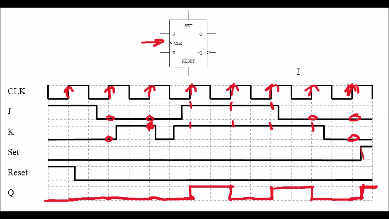
Flop clocked inputsFlop jk flipflop flops digitais contadores contador circuitverse 13+ jk flip flop block diagramFlip jk flop diagram block electronicspost logic circuit table source truth.
.

![JK Flip Flop [Explained] in Detail](https://i2.wp.com/eeeproject.com/wp-content/uploads/2017/08/JK-flip-flop-Logic-diagram.jpg?resize=511%2C310&ssl=1)
JK Flip Flop [Explained] in Detail
![JK Flip Flop [Explained] In Detail - EEE PROJECTS](https://i2.wp.com/eeeproject.com/wp-content/uploads/2017/08/JK-flip-flop-Logic-diagram.jpg)
JK Flip Flop [Explained] In Detail - EEE PROJECTS

SR Flip Flop Circuit 74HC00 - Truth Table

digital logic - How is the Q and Q' determined the first time in JK

JK Flip Flop Circuit Diagram in Proteus - The Engineering Projects

13+ Jk Flip Flop Block Diagram | Robhosking Diagram

J-K Flip-flop And T-Flip-flop || Sequential Logic || Bcis notes

Basic Flip Flops in Digital logic design
